There are a multitude of circumstances that make power conversion a necessity. Power conversion, of course, is the converting of electric power from one form to another, from one voltage to another, or one frequency to another; it also encompasses any/all combinations of these.
Power conversion can take various forms:
At the heart of any power-conversion scheme are fast-switching power semiconductor devices to enable the conversion in the most efficient manner. These devices typically operate at switching frequencies from 1 to 100 kHz. Note that power conversion does not encompass typical 50/60-Hz core/coil devices such as conventional utility step-up or distribution transformers.
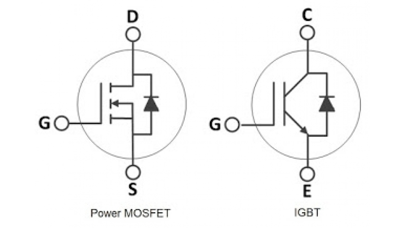
The mainstay building blocks of power conversion are the power MOSFET and the IGBT (Figure 1). These devices both operate in essentially the same way: a gate drive controls switching of current that flows between the drain and source (in the power MOSFET) or the collector and emitter (in the IGBT).
 |
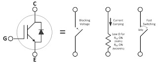
| Figure 2: Power semiconductors are very fast- switching devices with high blocking voltages and low forward-voltage drops |
In the context of a power-conversion system, the power semiconductor can be thought of as a very fast switch that can withstand a rated blocking voltage, typically in the hundreds of volts or even more than 1 kV. They can conduct a large amount of current with very low resistance (low forward-voltage drop). Switching rates are in the kilohertz range (Figure 2).
As mentioned earlier, switching in the power-semiconductor device is controlled through the gate-drive signal. A pulse-width-modulated (PWM) signal is applied to the device's gate lead to control the switching. This signal, which is typically from 3 to 24 V in amplitude, activates the device's switching at the rate governed by the gate-drive signal (Figure 3). Thus, a low-voltage signal on the gate drive controls switching of very high voltages on the output side of the device.
 |
| Figure 3: The gate-drive signal controls the switching activity of the power semiconductor |
Because the gate-drive signal is floating at the full (or half, depending on topology) DC bus voltage, there are some probing concerns. For very low-voltage drives of ~50 V or less, passive probes might be feasible. For higher voltages, use a high-voltage differential probe with isolation of 1000 VRMS from channel to channel and from channel to ground. Connecting a passive probe to a 600-V inverter circuit to look at the gate-drive signal will not turn out well for your oscilloscope.
In our next post, we'll look at considerations regarding the efficiency of power semiconductor devices and also look more closely at the devices themselves and how/where they're best used in conversion circuits.
Kaynak: https://blog.teledynelecroy.com/2019/10/basics-of-power-conversion-power.html